SEMICONDUCTOR TEST SOLUTIONS
Reduce probe costs by minimizing the number of touchdowns required to fully characterize each die. Cenfire switches enable signal paths to be reconfigured and sensitive measurements to be isolated directly on the probe card, allowing more test coverage within a single touchdown.
Improve tester resource utilization, reduce test time, and increase confidence in known good die before they are integrated into system in package assemblies. The result is lower test cost, improved yield visibility, and reduced SiP cost of goods sold.
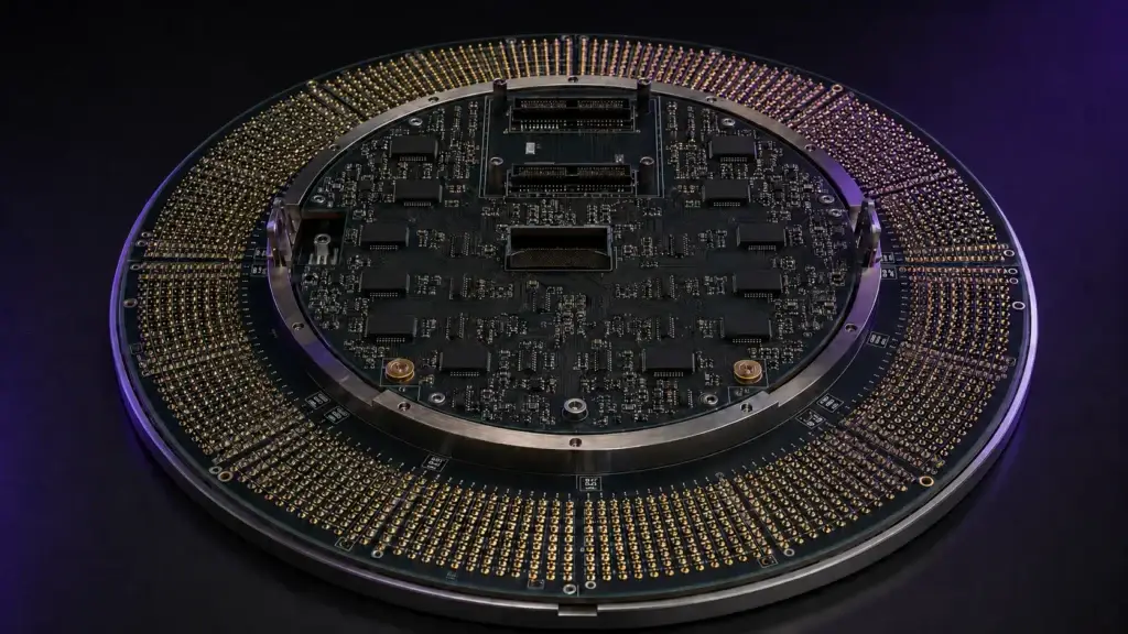
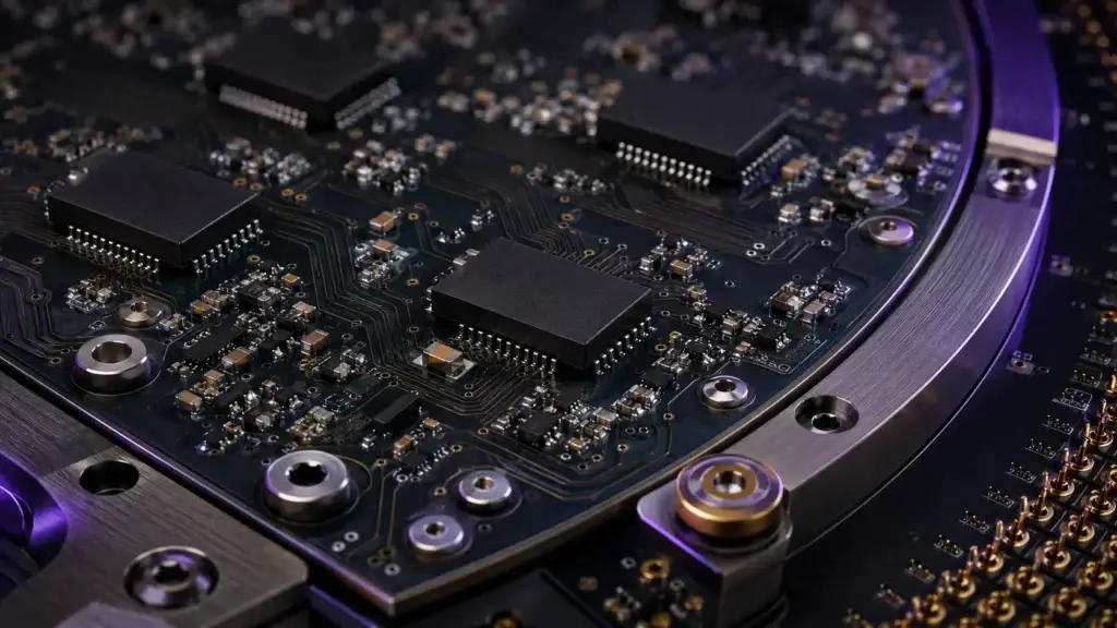
Every wafer touchdown consumes valuable probe-card life, tester time, and production capacity. When different measurements require separate signal paths, instruments, or test systems, the same wafer may need to be probed multiple times.
The CF2140 enables test paths to be reconfigured and isolated directly on the probe card, allowing more measurements to be completed during the same touchdown. Engineers can route DUT connections to different tester resources without physically changing the probe interface or making additional passes across the wafer.
Use compact, galvanically isolated switching to reconfigure DUT connections throughout the test sequence, allowing more measurements to be completed through the same probe-card interface.
Route DUT connections to different instruments and measurement paths without changing the physical probe interface. Four independently controlled SPST channels can also be configured as 2 × SPDT or 1 × SP4T for application-specific routing.
Disconnect inactive circuitry with true galvanic isolation. Leakage below 1 nA at 50 V helps prevent unwanted current paths from degrading high-impedance and low-current measurements.
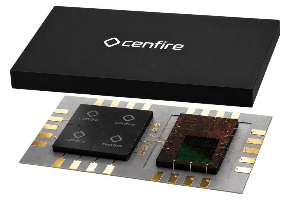
Integrate four independently controlled switching channels in a single compact package. An internal charge pump and standard 3.3 V digital control eliminate the need for separate high-voltage MEMS drive circuitry.
Complete more tests during the same touchdown and reduce the need to move a wafer between testers or make multiple passes on the same system. Fewer touchdowns can reduce test time, probe-card wear, and cost per die.
Route shared instruments to the DUT connections that need them instead of dedicating a separate tester resource to every measurement path. This enables more efficient use of available tester channels and instrumentation.
The CF2140 combines galvanically isolated signal routing, low leakage, low parasitic capacitance, and fast switching in a compact package designed for integration directly on the probe card
Independently connect or disconnect four DUT signal paths. The channels can also be configured as 2 × SPDT or 1 × SP4T to support signal selection, instrument sharing, and application-specific routing.
Minimize measurement error from current flowing through disconnected paths during high-impedance and low-current testing.
Avoid loading your signal path with unwanted capacitance when the switches are off—the open-channel capacitance remains essentially constant with voltage and does not vary with AC signal swing like a reverse-biased junction.
Reconfigure signal paths between test steps without the millisecond-scale delays associated with many mechanical relays, enabling rapid switching between ultra-fast tests that would otherwise require multiple passes when relay switching time exceeds the test duration.
Simplify Signal Routing
Route DUT connections to different instruments, isolate unused circuitry, and reconfigure measurement paths throughout the test sequence without changing the physical probe interface without juggling multiple relay types for different voltage levels, managing noise from relay coils, or dealing with the heat and inefficiency of discrete Darlington driver circuits.
Increase Probe-Card Capability
Support more test conditions and complete more measurements within each touchdown, reducing the need for separate probe-card designs, repeated wafer passes, or external switching systems, ultimately lowering total cost of goods by improving throughput, minimizing capital and operational expenses, reducing RMA costs, and avoiding losses from multi-die packages where a single failing die would otherwise require scrapping the entire package.
Consolidate the Switching Architecture
Replace multiple discrete switches and their supporting drive circuitry with four independently controlled, galvanically isolated channels in one compact package, reducing total cost of ownership through higher reliability, smaller board sizes, and significantly lower system downtime.