SEMICONDUCTOR TEST SOLUTIONS
Integrate fast, galvanically isolated MEMS switching directly onto load boards and DIB boards to increase test coverage, improve throughput, and simplify board design.
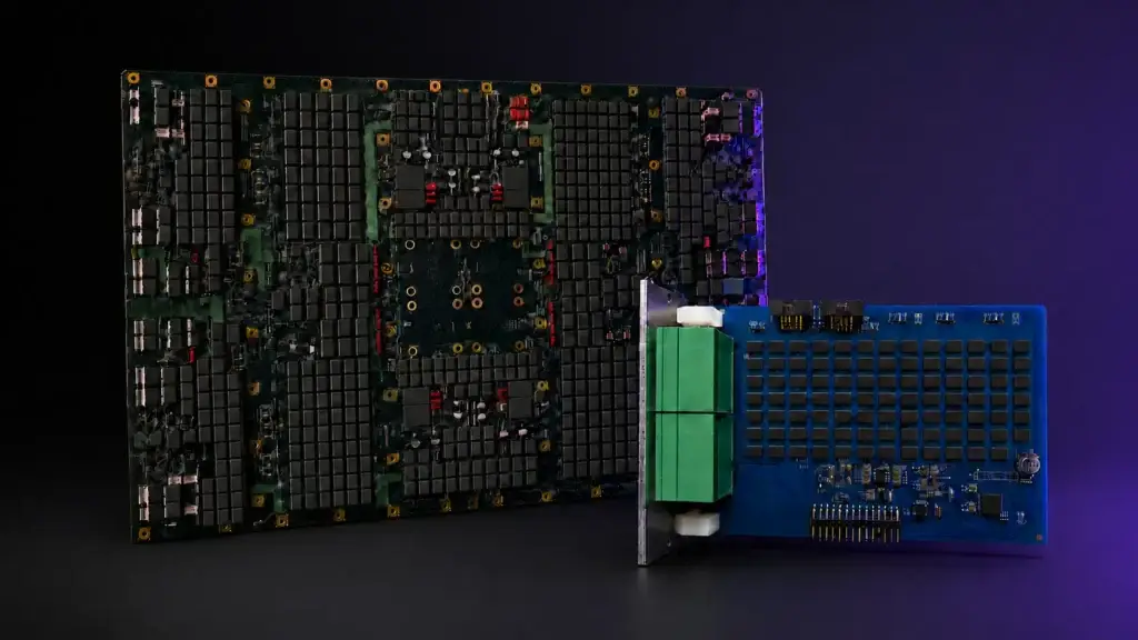
As semiconductor devices become more complex, load boards and device interface boards must support more signals, test conditions, and parallel test requirements. Traditional relay architectures make this difficult by consuming board space, requiring additional drive circuitry, generating heat, and delaying transitions between test conditions.
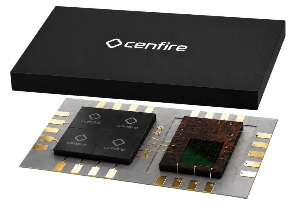
The Cenfire CF2140 brings fast, galvanically isolated switching directly onto the load board or DIB board. Four independently controlled SPST channels, 10 µs switching, and integrated 3.3 V digital control help test engineers:
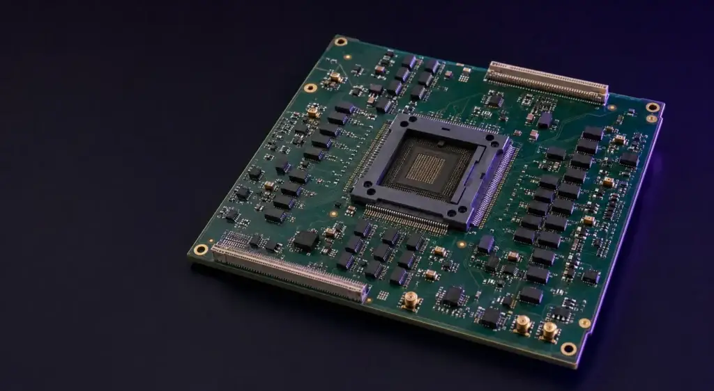
Integrate switching closer to the DUT to reduce board capacitance and inductances and eliminate the need for long cables and connectors. Additionally, overcome the size, speed, and control limitations of traditional relay architectures.
Add more switching directly onto the load board or DIB board to support additional signals and test conditions within the available board area.
Control four isolated SPST channels using SPI or parallel GPIO. If you need to individually control many switches, just daisy chain our devices and run them with a single SPI interface. The integrated charge pump eliminates the need for separate high-voltage relay drive circuitry and the noise associated with driving a relay coil.
Transition between test conditions in 10 µs to reduce switching delays and help enable more testing within a single touchdown. Your fast test times can now be accommodated with a fast enough switch without the MUX limitations on capacitance and breakdown voltages.
True galvanic isolation, less than 1 nA leakage at 50 V, and 0.2 pF typical parasitic capacitance support sensitive DC, analog, and high-frequency signal routing. Conduct your signal through a metallic path instead of relying on electrons or holes. There are no junctions in this device so your negligible capacitance doesn't change with input/output voltages (optimized linearity).
The CF2140 combines switching speed, isolation, density, and digital control in a compact package designed for integration onto semiconductor load boards and DIB boards.
Move rapidly between test conditions and reduce delays caused by traditional mechanical switching.
Maintain isolation across sensitive measurement paths and high-impedance test applications.
Route DC, analog, RF, and high-speed signals through one switching platform.
Integrate four isolated SPST channels onto space-constrained load boards and DIB boards.
Avoid a Costly Redesign
Increase switching density, accelerate test-state changes, and simplify signal routing directly on the load board or DIB board. Achieve the fastest time to yield on your design.
Protect Throughput and Time to Market
Improve throughput and test coverage while reducing the capital expense associated with board complexity and supporting test hardware. Get rid of costly RMAs without increasing your COGS.
Control BOM and Lifetime Costs
Lower operating expense by reducing power consumption, component count, relay replacements, maintenance, and downtime. Achieve significant TCO reduction on your projects.